
Loading...
Postulate is the best way to take and share notes for classes, research, and other learning.
Lecture 25: PCB design
 Samson Zhang
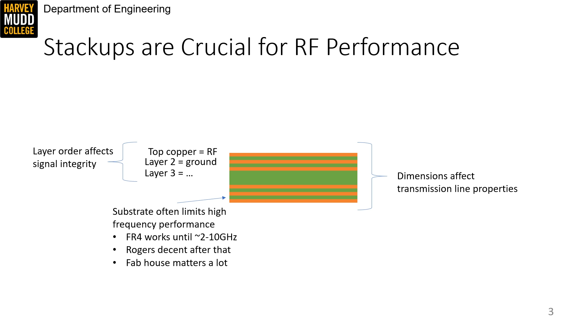
This is a stackup. Three things matter.
- Order of layers to make sure signals don't interfere with one another. Specifically HF and power planes should be adjacent to ground planes, while LF can go on non-critical planes.
- Substrate material. FR4 is cheap and easy to manufacture with but only works until 2-10 GHz. Rogers ceramic laminate has lower loss but is fragile and more expensive. The specific fab house also makes a big difference
- The distance between plates affects capacitance and inductance between traces
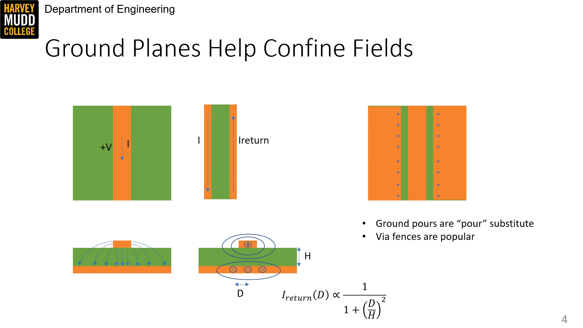
Ground planes closer to traces is better because it constrains the return path E and B fields and prevents spillover on the same layer of the trace. If a ground plane is impossible, ground pours can be used with vias to ground.
Transmission lines
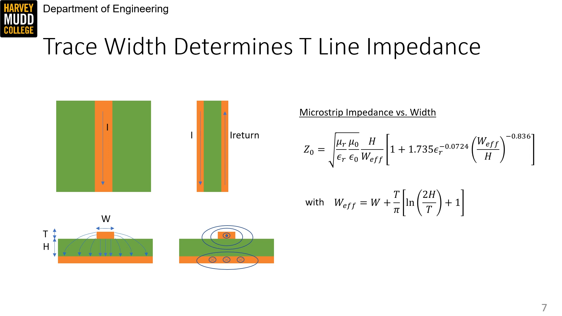
Transmission lines are useful for RF as well as high speed digital signals. Microstrips are one type, as well as striplines and coplanar waveguides.
There is an inductance-capacitance tradeoff in design.
- More separation between plates means more B field but less E field.
- Wider traces mean more E field coupling => capacitance, but less magnetic field => inductance.
There are many approximation equations for characteristic impedance of microstrip.
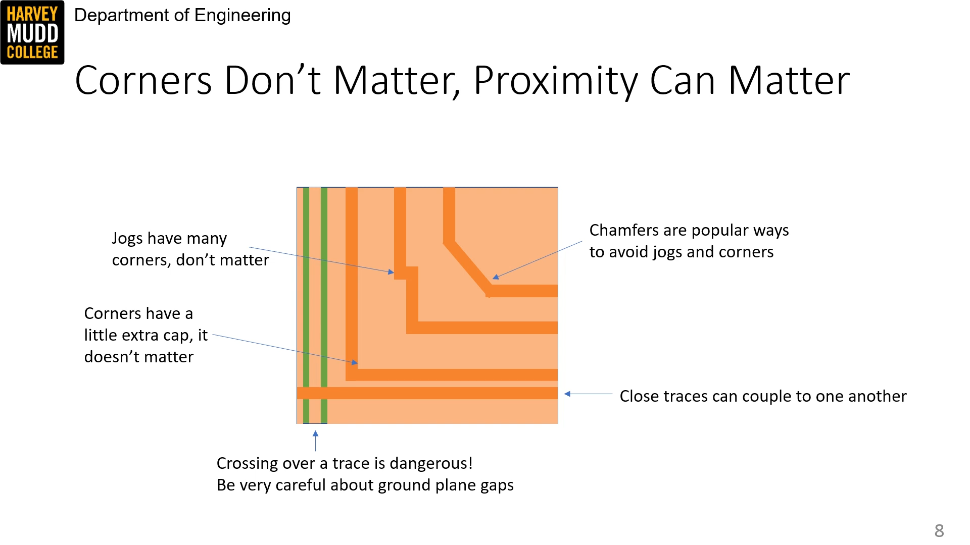
Corners don't matter until getting into the 10s of GHzs but there are strong aesthetic preferences in design -- use chamfers to avoid 90 degree turns.
Don't space traces too close together or have them cross over underlying traces or ground plane gaps. That can great coupling or parasitic capacitance.
Components and connectors
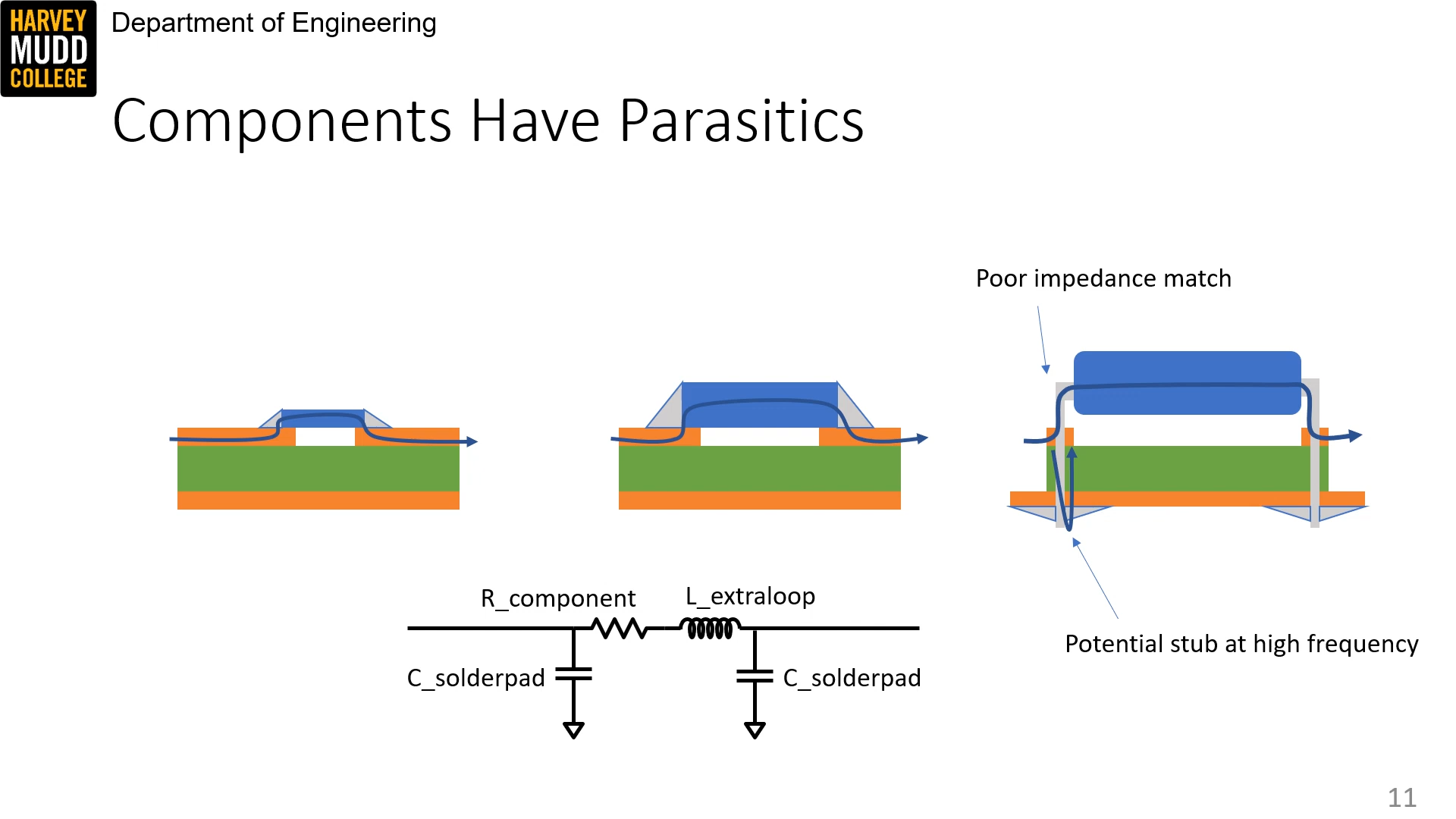
Components introduce parasitic capacitance and inductance. The bigger the component, the more parasitics. Through hole components are especially bad because of large solder pads and stubs.
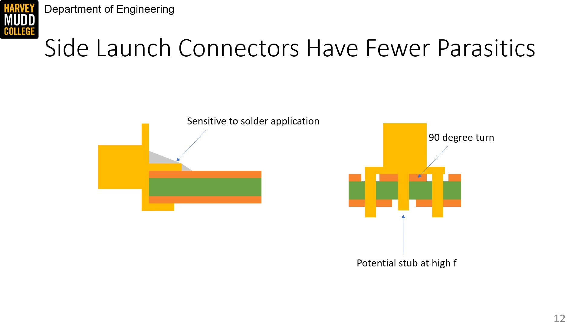
Connectors are also common failure points because it's where two transmission lines meet. Side launch is generally better than vertical.
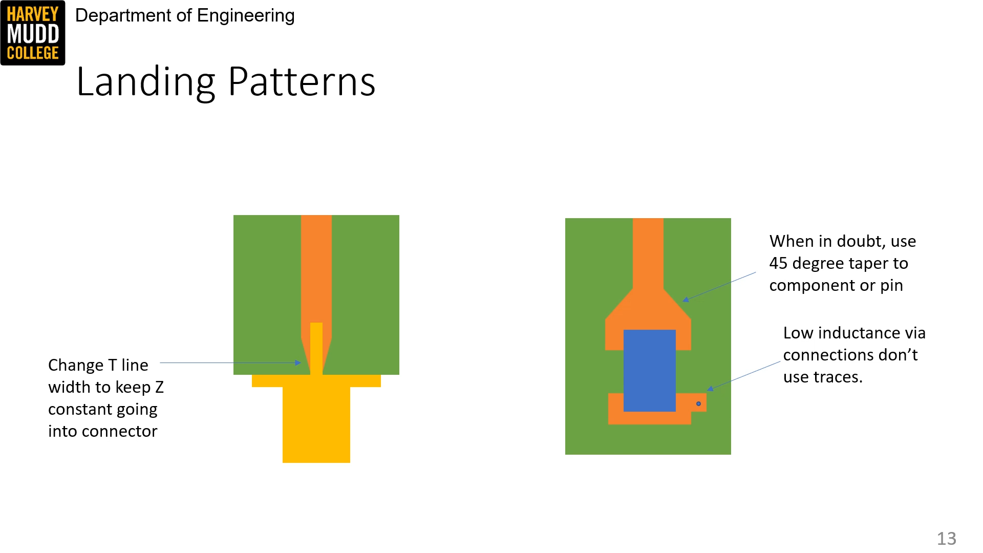
Landing patterns, how the microstrip/trace changes to allow a component to be attached to it, matter because they change the line impedance. They need to be carefully designed. Tapers help.
Vias are sensitive to layout -- extra length is bad because it creates parasitic inductance.
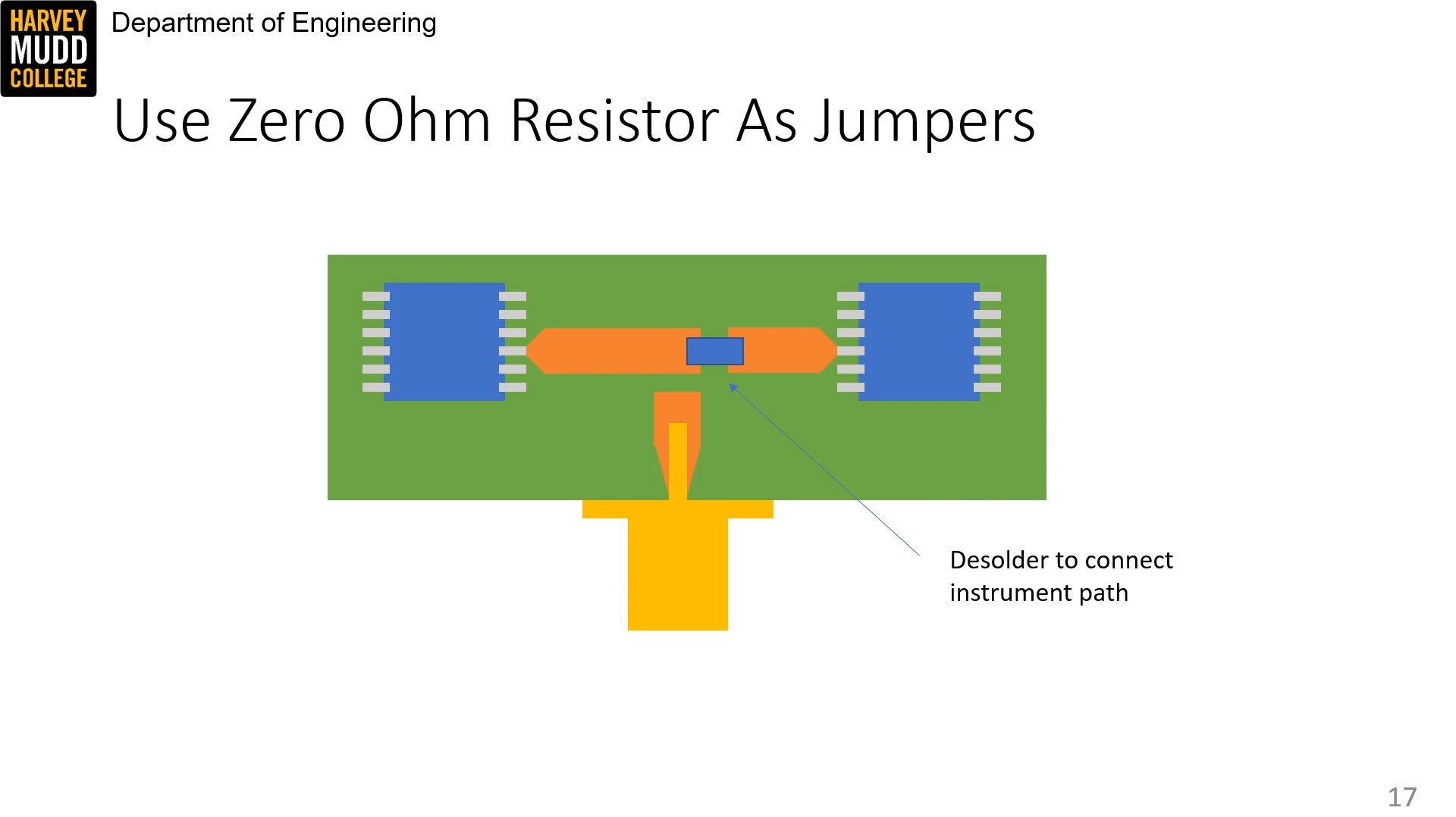
0 ohm resistors for debugging
You can't debug RF by just looping a measurement in along a transmission line -- that creates impedance mismatch, or, when the measurement instrument is disconnected, a stub to an open.
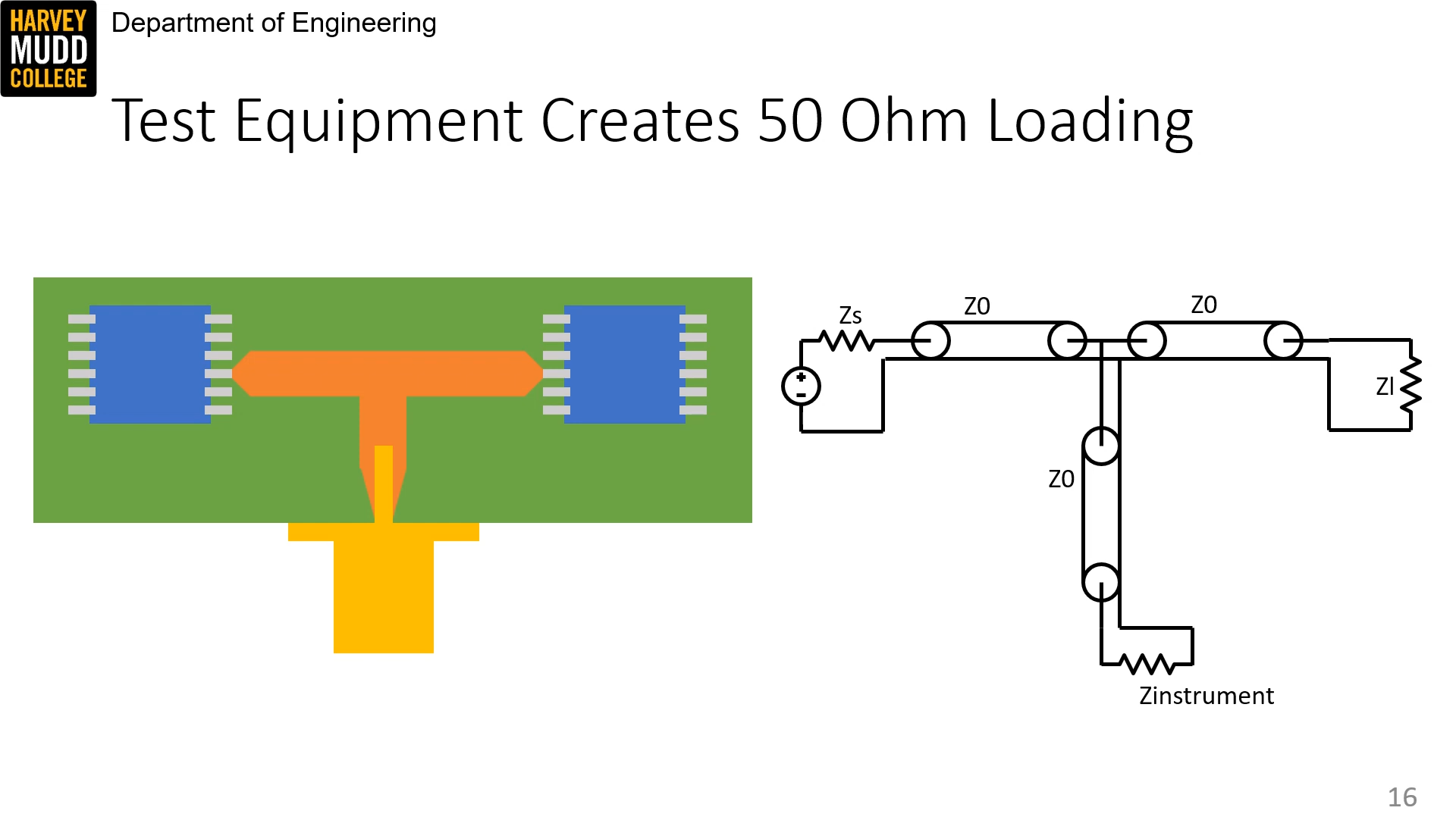
Instead, use 0 ohm resistors and solder/desolder them to reconfigure a circuit for debugging.
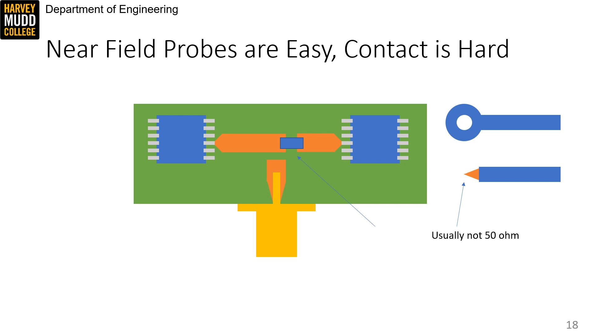
Near-field probes are easy to use with RF but contact probes aren't (like for oscilloscope) because they have very high impedance -- don't really interfere with circuit but also don't pick up much signal.
Comments (loading...)
e157: radio frequency circuit design
fall 2023 class w prof. spencer